High-Efficiency Solar cells
2018-2019
I worked as a Research intern in the III-V Solar cells group at Fraunhofer ISE. The focus of my research was to support the methods to reduce the cost of production of ultra-high-efficiency solar cells. If the cost of high-efficiency solar cells comes down, they have enormous potential to power space-constraint products like fixed-wing UAVs, IOT sensors.
Problem : Despite the shorter band gap of III-V group Solar cells, the advantage is negated by the high production cost of III-V semiconductor technology. The GaAs substrate material used for the development of III-V group solar cells cannot be reused after growing the solar cell layer. A 6-inch wafer typically costs $100, and thus this makes it a commercially non-viable solution.
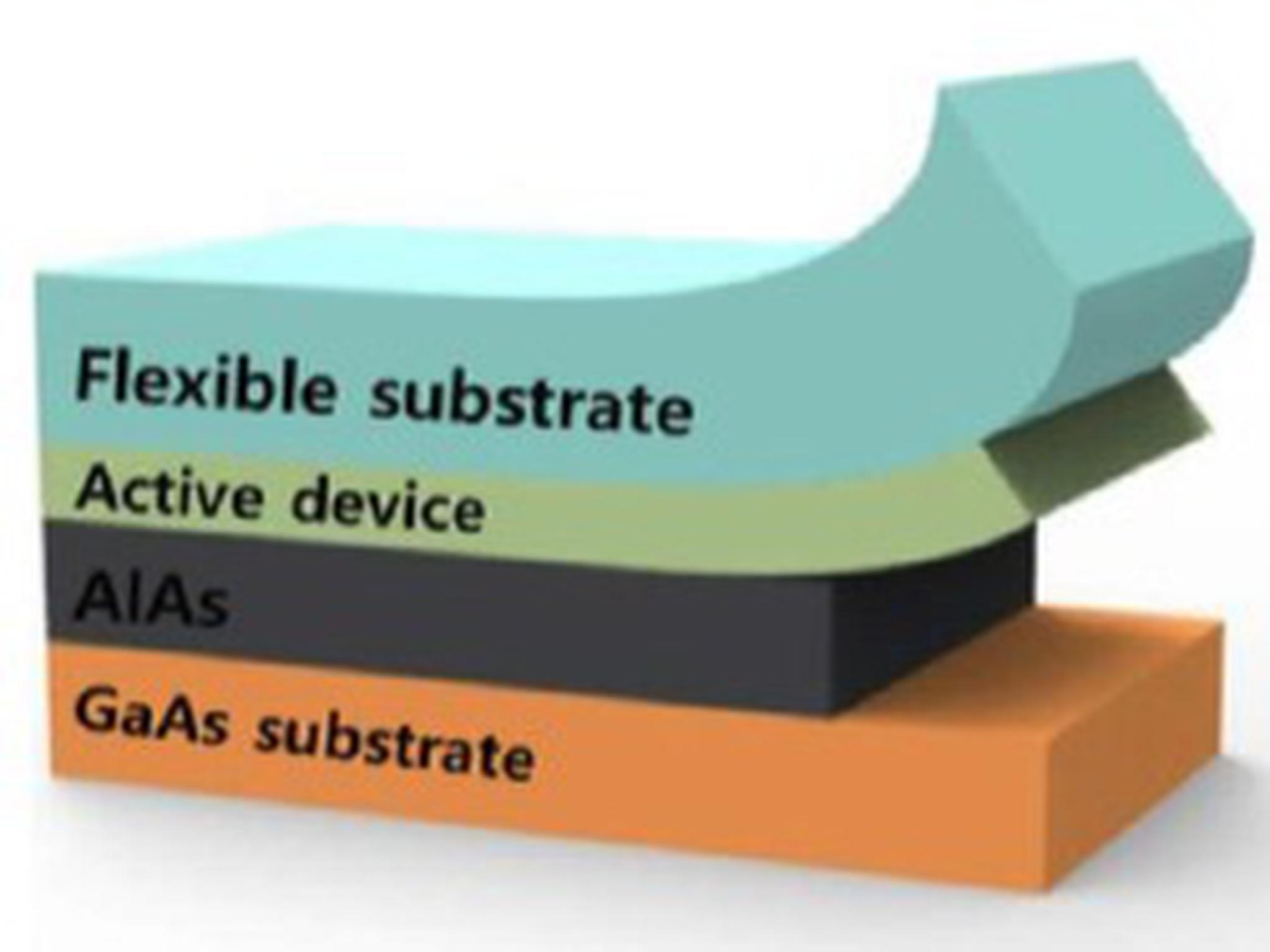
Solution : With a new processing technology approach, an AlAs sacrificial layer is deposited over the substrate and then the solar cell layer is grown over that sacrificial layer. Using the process called Epitaxial Lift-Off (ELO), this entire combination is dipped into HF, and then the sacrificial layer is etched away, giving us the solar cell and the substrate. Now this substrate can be reused and the solar cell can be used for further processing.
Contribution : During my internship, I primarily worked on studying methods that might help in reusing GaAs substrate :
-
Epitaxial Lift Off (ELO) : Worked on the state-of-the-art ELO process. Performed ELO of the new solar cell samples in an HF bath under different concentration and time parameters.
-
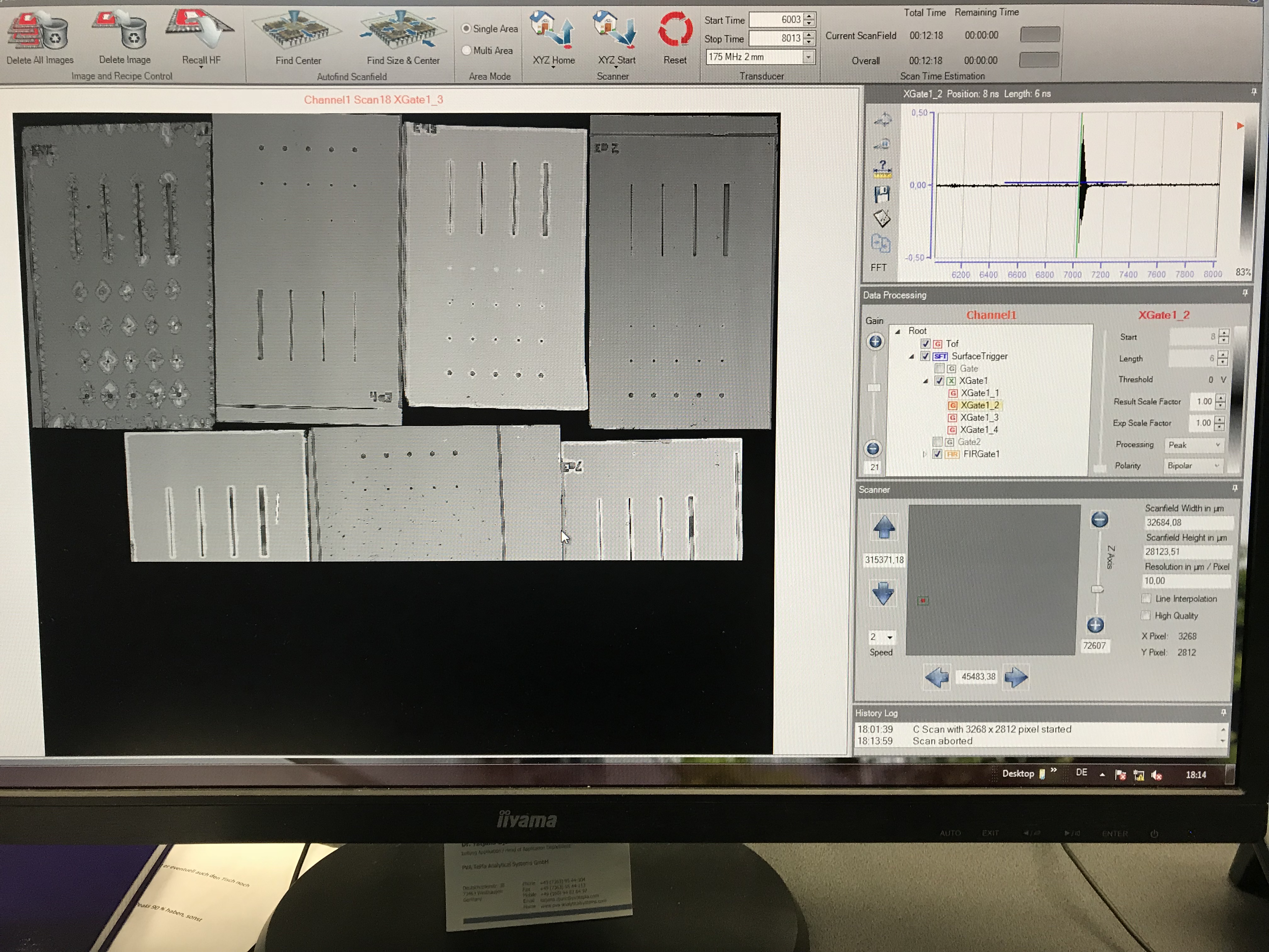
Measurements using Scanning Acoustic Microscope (SAM) : Measured and evaluated the newly processed samples using SAM to get information about the etching behaviour of sacrificial layers in different conditions, find defects and the material quality of the layers.
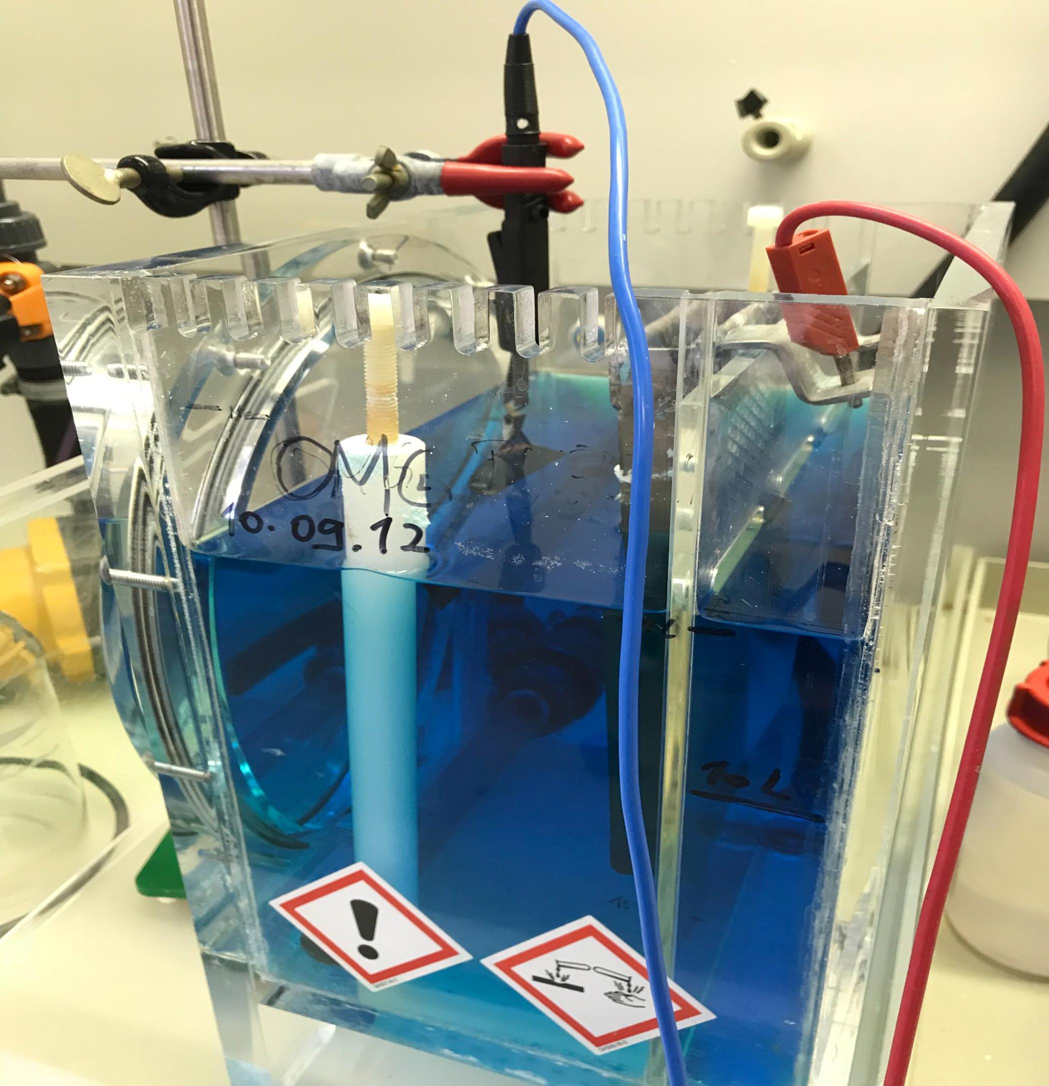
- I worked on the electrochemical deposition of Ni/Cu contacts on the very thin solar cell layer that is generated after the ELO process. This contact deposition is done to make the μm thin solar cell layer stable and use the contacts for further characterisation.
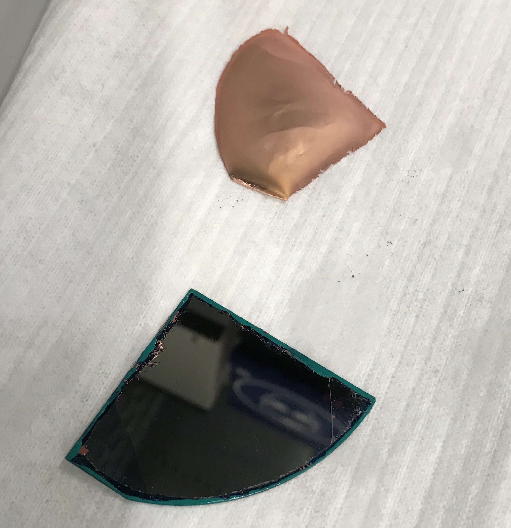
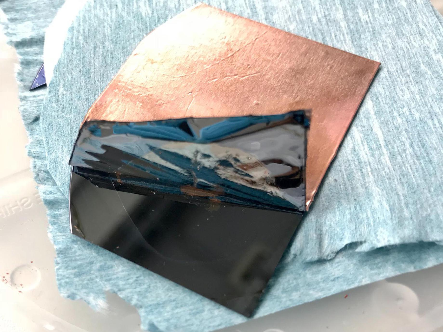
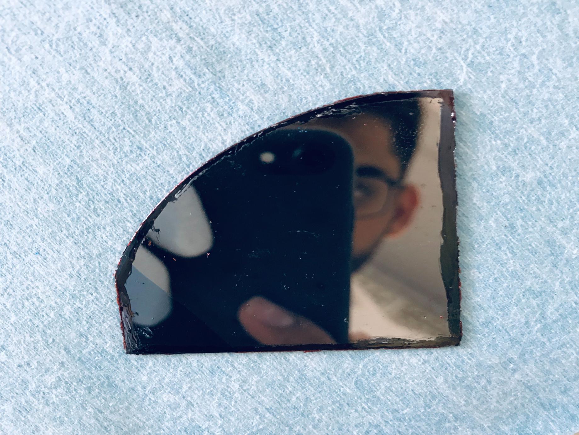
- Experimented with different potential options for temporary substrates of solar cells, instead of conventional Ni/Cu plating. I found electrically conductive CU tape as a better alternative to the existing Ni/Cu plating in terms of both time and cost of processing. I experimented by pasting the tape on the solar cell layer material and annealing this sample. The results were comparable to the Ni/Cu plating method. With this cheaper substrate, it became possible to quickly evaluate new solar cells with different layer compositions.
Project Supervisor : Dr. Frank Dimroth
Work Funded by : Fraunhofer ISE and Delhi Technological University’s Alumni Network